Jason Dunlap has more than 25 years of experience designing RF and Microwave PC boards. He has done designs for notable companies such as, Anritsu, Agilent Technologies, NetworkFab, and military contractors.
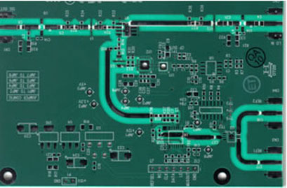
Field solvers, ADS simulator and other software gives the RF engineer the answer to complicated and theoretical considerations needed to do circuit board layout correctly, but ultimately the PCB designer must have the skill and know-how to implement the engineer’s requirements. As in the circuit board shown here, removal of the solder resist material was necessary. Solder resist material can cause losses. This was also done in order to mask off certain areas to aid in troubleshooting and if needed, to solder on more components during RF optimization of the prototype.

We know to ask the right questions, in order to be sure we are designing to your standards, and not our own. Using desktop sharing, your engineer can show the designer exactly how they want it, just as if they were sitting beside them.

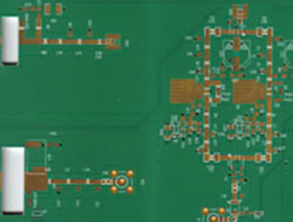
This design required special attention to via placement and the use of blind vias because only ground vias were allowed to penetrate to the bottom layer. The bottom layer was attached to a heat sink. This design also required special attention to via placement and the use of blind vias because only ground vias were allowed to penetrate to the bottom layer. The bottom layer was attached to a heat sink. Therefore, signal vias were blind vias so they wouldn’t short to the heat sink. Another, less costly solution could have been to map the vias, and back drill those vias that were not ground nets.
This design required special attention to via placement and the use of blind vias because only ground vias were allowed to penetrate to the bottom layer. The bottom layer was attached to a heat sink. This design also required special attention to via placement and the use of blind vias because only ground vias were allowed to penetrate to the bottom layer. The bottom layer was attached to a heat sink. Therefore, signal vias were blind vias so they wouldn’t short to the heat sink. Another, less costly solution could have been to map the vias, and back drill those vias that were not ground nets.
High frequency RF designs require special attention to details, and the designer needs to work closely with the RF engineer in order to follow all instructions. Most RF designs are 100% hand-routed. Special attention to impedance controlled stackups is also important and we often suggest mixed materials such as Rogers 4003 and FR408. In high-layer count designs, some creativity may be required to meet desired trace widths, where adjacent layers are very close. Finally, your designer will place comprehensive notes on the fabrication drawing and instruct the manufacturer about special requirements.